A semiconductor diode is a two terminals nonlinear circuit element. It has non-linear V-I characteristics whereas the resistor has a linear relationship.
A P-N junction is formed by simply joining a p-type material and an n-type material together. The semiconductor diode is made by biasing the P-N junction.
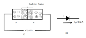
Figure: (a) P-N junction (b) Diode Symbol and direction.
Joining a p-type material (holes as a majority carrier) with an n-type material (electrons as a majority carrier) and no bias is applied to its terminal; this creates a depletion region between the P-N junctions due to its charge carrier. There is no current flow and diode voltage is zero.
Figure: (a) Charge distribution under no applied bias (b) Diode symbol and direction.
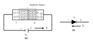
Reverse bias is introduced by applying an external voltage such that the positive terminal is connected to the n-type material and the negative terminal is connected to the p-type material. The negative potential to the p-type material and the positive terminal to the n-type material creates a large number of negative ions and positive ions respectively.
The depletion region becomes wider and there is no majority carrier flow. Reverse bias current flows due to the majority carrier and it is called reverse saturation current Is.
Figure: (a) Internal distribution of charge under reverse bias condition (b) Diode symbol and direction.
Forward bias is created by applying an external voltage such that the positive terminal is connected to the p-type material and the negative terminal is connected to the n-type material. The depletion region is smaller because of the majority carrier flow.
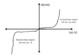
The positive and negative potential to the p-type material and n-type material breaks the charge barrier and the diode current flow. The characteristic of a diode is determined by the Shockley’s equation:
ID= IS (e^(Vd/nVt) -1) A
Where,
- ID=Diode current
- IS=Reverse saturation current
- Vd =Externally applied voltage
- n= Ideality factor
- Vt= Thermal voltage
Figure: Si semiconductor diode characteristics
The thermal voltage is determined by
Vt= (KTk/q) (v)
Where,
- K= Boltzmann’s constant= 1.38˟10-23J/K
- Tk= Absolute temperature in kelvin = 273+̊C
- q= Magnitude of electronic charge= 1.6˟10-19C.
Q. At a temperature 27̊C, determine the thermal voltage Vt.
Solution:
Tk= (273+27)K=300 K
Vt= KTk/q =(1.38˟10-23 ˟ 300)/1.6˟10-19 =25.875 mV=26 mV
Table of Contents
Application of semiconductor diode:
Diode is generally used as
- Rectifier
- Clipper
- Clamper
- Voltage multiplier
- Logic gate maker
For the reverse bias potential in a diode, there is a sharp change in the voltage-current relationship. The current increases at a very rapid rate in the negative voltage region. The reverse bias potential draws an abrupt change in the characteristics curve is called breakdown potential VBV. This occurs because the valance electrons absorb the sufficient energy to leave the parent atom (called ionization process).
The sharp change in the characteristics at any level of the negative potential is called the Zener region. Zener Breakdown occurs because there is a strong electric field in the region of the junction that can disrupt the bonding forces within the atom and generate carriers.
The maximum reverse bias potential that can be applied before entering the Breakdown region is called the peak inverse voltage (PIV) or the peak reverse voltage (PRV).
Different semiconductor diode starts to flow current at a different maximum forward bias potential, which is called knee voltage Vk.
Table: Knee voltage of semiconductor diode
| Semiconductor | Vk(V) |
| Ge | 0.3 |
| Si | 0.7 |
| GaAs | 1.2 |
Temperature effect
In the forward bias region the characteristics of a silicon diode shift to the left at a rate of 2.5 mV per centigrade degree increase in temperature. In the reverse bias region the reverse current of a silicon diode double for every 10 degrees centigrade rise in temperature.
The semiconductor diode acts as a switch. The only difference is that the diode current flows in one direction whereas a switch allows the current flow in both directions.
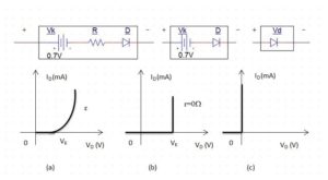
Diode equivalent circuit:
Figure: (a) Piece-wise linear equivalent circuit (b) Simplified equivalent circuit (c) Ideal equivalent circuit.
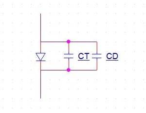
The transition capacitance is the predominant capacitive effect in the reverse bias region whereas the diffusion capacitance is the predominant capacitive effect in the forward bias region.
Figure: Transition and diffusion capacitance in the semiconductor diode.
Zener diode:
Diode showing the sharp change in the characteristics of a P-N junction is called Zener diode. The higher is the number of adding impurities the lower is the Zener potential. Zener diode is always set to the reverse biased.
Figure: Zener diode characteristics, symbol and direction.
Application of Zener diode:
- As a voltage regulator
- As a protective device
- To generate a square wave
- To use in a transistor circuit
Difference between a conventional diode and a Zener diode:
| Diode | Zener diode |
| It has no definite breakdown voltage. | It has a Zener voltage. |
| It has slightly less impurity material than Zener impurity. | It contains much more impurities than conventional diode impurities. |
| It does not work at Breakdown region. | It works in the breakdown region. |
| It is connected at forward bias in a circuit. | It is connected at reverse Biased only. |
| It is damaged by the application of extra peak inverse voltage. | It is conducted at a certain amount of reverse voltage. |
LED (light Emitting Diode)
One types of diode that glow visible lights
- It converts the forward current into light.
- At the modified p-n junction of the LED, the electron changes its energy level; then the energy is transformed into heat and photon.
SBD (Schottky-Barrier Diode)
The SBD is formed by bringing material into contact with a moderately doped n-type semiconductor material.
- The diode current flows from the metal anode to the semiconductor cathode.
- The diode acts as an open circuit in the other.
- The current is conducted by majority carriers (electrons).
- The forward voltage drop of a conducting SBD is lower than that of a p-n junction diode.
- Metal is commonly deposited on the semiconductor surface in order to make terminals for the semiconductor devices and to connect different devices in an integrated circuit chip.
Diode Testing
- By Digital Display Meter (DDM): Determining the ‘ON’ state by estimating the specific diode forward bias voltage.
- By Ohmmeter Testing: Determining the resistivity for relatively low (short circuit) or high (open circuit) value with ‘ON’ or ‘OFF’ state respectively. The ‘ON’ state shows its polarity.
- By Curve Tracer: Tracing diode characteristic curve by positioning the exact polarity (ON) mode.
Analyze yourself:
| Q1. What do you mean by diode? Draw the diode characteristic curve. |
| Q2. What is a p-n junction? Describe reversed biasing. |
| Q3. Define the Zener region, Breakdown voltage, PIV, Knee voltage. Write down the uses of a diode. |
| Q4. Draw the diode equivalent circuits. Distinguish between switch and diode. |
| Q4. Broadly explain the Zener diode. Differentiate between Zener diode & conventional diode. |
| Q5. Write a short note on 1. LED 2. SBD 3. Diode testing |


